In this tutorial, we will be generating some audio tones using the FPGA.
OK. First thing is to understand what constitutes a tone and how it can be generated digitally. Basically, a tone is a periodic audio signal. A speaker or a earphone coverts an electrical waveform into an audio signal of the same frequency and proportionate amplitude. So, our job is to generate a voltage(analog) signal to drive the output device.
Also if a single analog output is generated, then it is called mono. If 2(or more) outputs are generated – one for each earphone lead/speaker, then it is called stereo.
We need a mechanism to convert the digital data in the FPGA to analog waveform. Ideally, we need a DAC(Digital to Analog covertor) to do the conversion. But the board lacks a dedicated DAC; hence we have to make do with a ‘PWM DAC’. 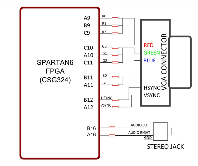
As you can see. the FPGA pins are connected to 2 resistors and then to the output.
What is PWM?
PWM stands for pulse width modulation. Its a powerful technique used in a variety of ways. One popular use case is to use it generate a desired analog voltage.
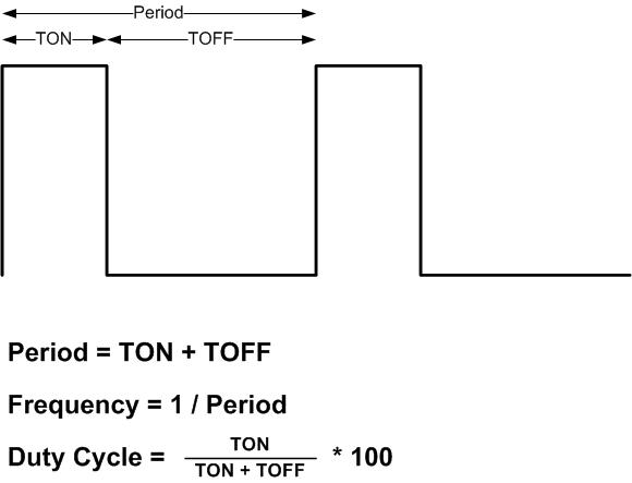
PWM is a periodic train of square pulses. The frequency of the pulses are fixed but the pulse width can vary between pulses. Lets say the high state is expressed as a voltage of +3.3v and zero state is 0v. If we compute the average voltage a cycle, it is,
Vavg = (3.3*Ton + 0*Toff)/period = 3.3 * Ton/period = 3.3*DC
where, DC is the fractional duty cycle = Ton/(Ton+Toff) = Ton/period
Thus you can control the average voltage output by controlling the Ton period. Thus if Ton is a quarter of a period, then Vavg = 3.3/4 = 0.825v.
So, how is it practically implemented? In a digital system, the Ton can take only discrete steps. Lets say we have Ton as a 8bit value and a 8bit counter register. The counter counts from 0-255 and then back to 0 and so on(free running). The period of the counter register is the PWM period. 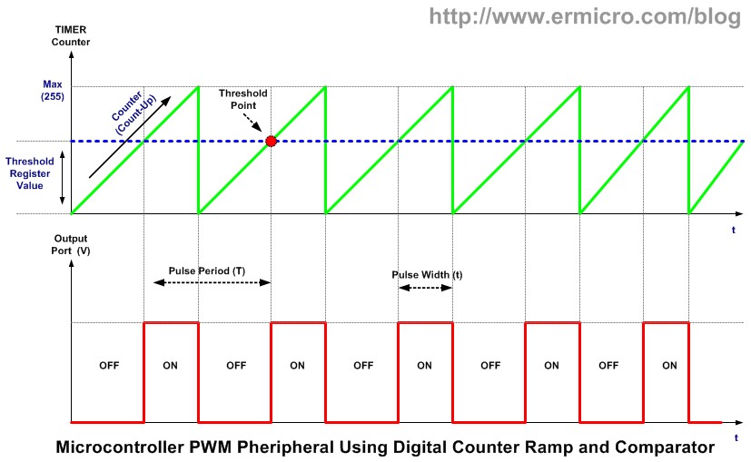
We can have a digital comparator which outputs ‘1’ if Ton<counter and ‘0’ if Ton>=counter. The Ton register can be set to any arbitrary value from 0(100% duty cycle) to 255(0% duty cycle). This is visualized in the picture above. The output of the comparator can be routed to an FPGA pin to the stereo jack.
In our system, there is just a slight modification. The conditions for the ‘1’ and ‘0’ are simply reversed.
What is sample rate?
The sample rate is the maximum rate at which the digital data samples for the audio ouput can be changed. That is, every sample period, a new data value can be put into the PWM comparator (Ton register). There are some standard audio sample rates one of which is 44Khz(which we will be using).
So we can put a new value to the PWM comparator reg every 1/44KHz = 22.727us. In this case our PWM frequency is the same as Sample rate = 44Khz.
We will end up with an ‘average’ waveform like this:
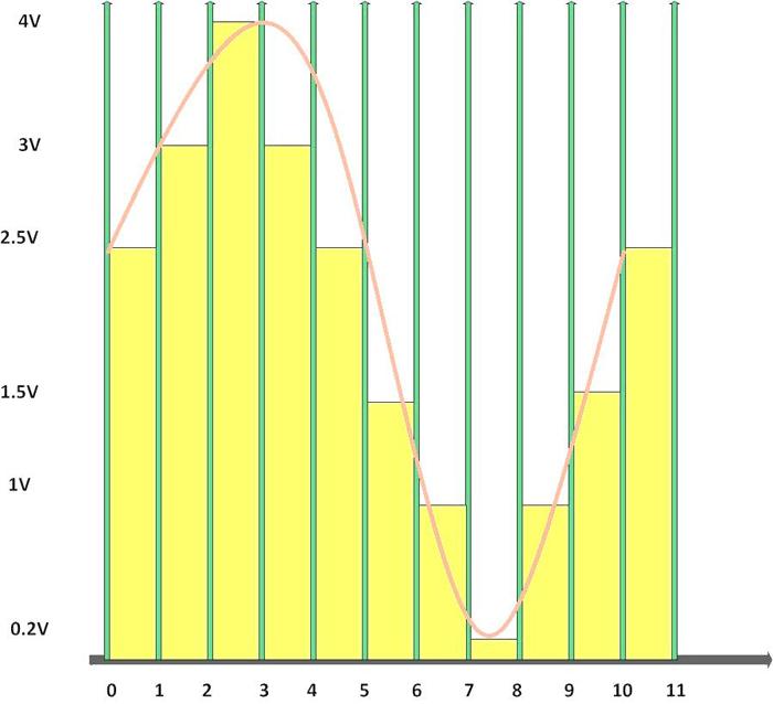
Notice that it changes in steps every sample period. Ideally for audio we prefer a continuous signal without discontinuities. To improve the audio quality we can do 2 things:
- one is to increase the sampling rate(and also PWM freq) so that the steps can be made more finer, making it closer to continuous waveform.
- Increase the PWM frequency keeping the sample rate same. An increased sample rate poses increased data processing loads on the system. But no such cost is incurred if you only increase the PWM frequency. This will make the output analog values closer to what you intended.
We are going to go with option 2. I chose the PWM frequency = 10*sample rate. Hence PWM freq = 440KHZ.
Also you might be wondering why PWM is called ‘modulation’. This because the message signal(our audio) is represented by the changing pulse widths of the high frequency carrier(PWM pulse train).
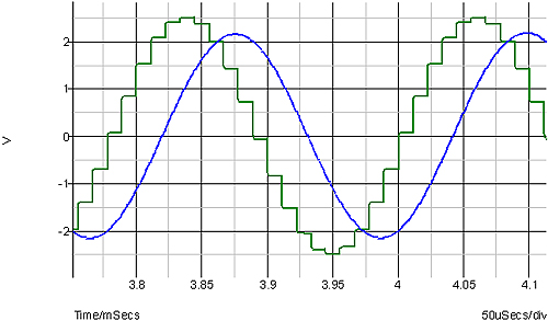
Finally, you should know that even though we have increased our PWM frequency ten fold, there may some audible artifacts because of the discontinuities in the output signal. To smoothen this out, a not so straight forward low pass filter is employed. The earphones/speakers internally contain capacitive components to block DC voltages. The resistor on the FPGA pin combined with this capacitance, form a simple RC low pass filter. The final output may look something like this.
Ok. With that theory base, the implementation is straight forward.
The system clock is 100MHz. We need to divide this with suitable counters to generate the PWM counter and the sample clock.
pwm divisor = 100M/440K = 227 (this is PWM counter period)
sample clock divisor = 100M/44K = 2273
The PWM counter counts from 0 to 226 and back to 0 and so on. Every sample clock, a new value is loaded into the Ton comparator reg.
So what values are we going to load into the Ton reg? A very crude sine wave consists of rising phase and falling phase. So I start with 0 and increment it by an amount ‘sampleInc’. Once it reaches 226, then it starts decrementing by ‘sampleInc’ amount till it reaches 0 and so on. The sampleInc value, I have kept it programmable through the serial interface. Note that higher sampleInc means the sine cycles get completed sooner – higher frequencies. The sampleInc gets displayed on the 7 segment display.
Both the left and right channels are driven by the same signal.
top_module.v
`timescale 1ns / 1ps

module top_module(L,R,a,b,c,d,e,f,g,h,e1,e2,e3,tx,rx,clk,reset);

output L,R;
output a,b,c,d,e,f,g,h,e1,e2,e3,tx;
input rx,clk,reset;

localparam [1:0] idle=2'b00, data1=2'b01, data2=2'b10, data3=2'b11;

// Signals for UART submodule
reg rd_uart = 1'b0;
reg wr_uart = 1'b0;
reg [7:0] data_out = 0 ;
wire [7:0] data_in ;
wire full ;
wire empty ;
reg [7:0] data_rx = 0 ;
reg [1:0] rx_state = 0 ;

reg [9:0] disp_num = 0 ;
reg [9:0] disp_num1 = 1'd1;
wire [3:0] dig0,dig1,dig2 ;
reg [3:0] currentDig ;
reg [1:0] digCnt = 2'd0 ;
reg dig0en,dig1en,dig2en;
assign e1=dig2en; assign e2=dig1en; assign e3=dig0en;

reg [15:0] timer_cnt = 0 ;
reg [7:0] pwmCnt = 0 ;
reg [11:0] sampCnt = 0 ;
reg sampClk = 0 ;
reg [7:0] sampleVal = 0 ;
reg [7:0] sampleInc = 8'd1;
reg IncDec = 1'b1;

assign L = sampleVal >= pwmCnt;
assign R = sampleVal >= pwmCnt;

bin2BCD v1({dig2,dig1,dig0},disp_num1);
BCDto7Seg v2(a,b,c,d,e,f,g,h,currentDig);

// DIVISOR = 326 for 19200 baudrate, 100MHz sys clock
uart #( .DIVISOR (9'd326),
.DVSR_BIT (4'd9) ,
.Data_Bits (4'd8) ,
.FIFO_Add_Bit (3'd4)
) uart ( .clk (clk),
.rd_uart (rd_uart) ,
.reset (reset) ,
.rx (rx) ,
.w_data (data_out) ,
.wr_uart (wr_uart) ,
.r_data (data_in) ,
.rx_empty (empty) ,
.tx (tx) ,
.tx_full (full)
);

// Timer logic
always @(posedge clk)
begin
if(!reset)
timer_cnt <= 0;
else
timer_cnt <= timer_cnt + 1'b1;
end

always @(posedge clk or negedge reset)
begin
if(!reset)
sampCnt<=0;
else if(sampCnt==12'd2272)
begin sampClk<=1'b1; sampCnt<=0; end
else
begin sampCnt<=sampCnt+1'b1; sampClk<=1'b0; end
end

always @(posedge clk or negedge reset)
begin
if(!reset)
pwmCnt<=0;
else if(pwmCnt==8'd226)
pwmCnt<=0;
else
pwmCnt=sampleInc)
sampleVal<=sampleVal+sampleInc;
else
IncDec=sampleInc)
sampleVal<=sampleVal-sampleInc;
else
IncDec<=1'b1;
end
end

always @(posedge timer_cnt[10] or negedge reset)
begin
if(!reset)
begin
rx_state<=idle;
disp_num<=0;
disp_num1<=10'd1;
sampleInc<=8'd1;
end
else
begin
if(!empty)
begin
rd_uart <= 1'b1;
data_rx ="0" && data_rx<="9") begin rx_state<=data1; disp_num="0" && data_rx<="9") begin rx_state<=data2; disp_num<=4'd10*disp_num + (data_rx-"0"); end
else if(data_rx=="\r") begin
rx_state=10'd1 && disp_num<=10'd100) begin disp_num1<=disp_num;sampleInc<=disp_num[7:0]; end
disp_num<=0; end
else begin rx_state<=idle; disp_num="0" && data_rx<="9") begin rx_state<=data3; disp_num<=4'd10*disp_num + (data_rx-"0"); end
else if(data_rx=="\r") begin
rx_state=10'd1 && disp_num<=10'd100) begin disp_num1<=disp_num;sampleInc<=disp_num[7:0]; end
disp_num<=0; end
else begin rx_state<=idle; disp_num<=0; end
end
data3: begin
if(data_rx!="\r") begin rx_state<=idle; disp_num<=0; end
else begin
rx_state=10'd1 && disp_num<=10'd100) begin disp_num1<=disp_num;sampleInc<=disp_num[7:0]; end
disp_num<=0; end
end
endcase
end
else
rd_uart<=1'b0;
end
end

always @(posedge timer_cnt[15]) begin
case (digCnt)
2'd0: begin
digCnt <= 2'd1;
dig2en <= 1'b1;dig1en <= 1'b1;dig0en <= 1'b0;
currentDig <= dig0;
end
2'd1: begin
digCnt <= 2'd2;
if(dig1==4'd0 & dig2==4'd0) begin dig2en <= 1'b1;dig1en <= 1'b1;dig0en <= 1'b1; end
else begin dig2en <= 1'b1;dig1en <= 1'b0;dig0en <= 1'b1; currentDig <= dig1; end
end
2'd2: begin
digCnt <= 2'd0;
if(dig2==4'd0) begin dig2en <= 1'b1;dig1en <= 1'b1;dig0en <= 1'b1; end
else begin dig2en <= 1'b0;dig1en <= 1'b1;dig0en <= 1'b1; currentDig <= dig2; end
end
endcase
end

endmodule
audioTest_ucf.ucf
#####################################################################
# Clock 100 MHz #
#####################################################################
CONFIG VCCAUX = "3.3" ;

NET "clk" LOC = V10 | IOSTANDARD = LVCMOS33 | PERIOD = 100MHz ;

#####################################################################
# Reset #
#####################################################################
NET "reset" LOC = M16 | IOSTANDARD = LVCMOS33 | DRIVE = 8 | SLEW = FAST | PULLUP; #SW3
NET "reset" CLOCK_DEDICATED_ROUTE = FALSE;

#####################################################################
# Uart #
#####################################################################
NET "tx" LOC = B8 | IOSTANDARD = LVCMOS33 | DRIVE = 8 | SLEW = FAST ;
NET "rx" LOC = A8 | IOSTANDARD = LVCMOS33 | DRIVE = 8 | SLEW = FAST ;

NET "L" LOC = B16 | IOSTANDARD = LVCMOS33 | DRIVE = 8 | SLEW = FAST ;
NET "R" LOC = A16 | IOSTANDARD = LVCMOS33 | DRIVE = 8 | SLEW = FAST ;

NET "a" LOC = A3 | IOSTANDARD = LVCMOS33 | DRIVE = 8 | SLEW = FAST ; #a IO_L4N_0 Sch = 7Seg_0
NET "b" LOC = B4 | IOSTANDARD = LVCMOS33 | DRIVE = 8 | SLEW = FAST ; #b IO_L5P_0 Sch = 7Seg_1
NET "c" LOC = A4 | IOSTANDARD = LVCMOS33 | DRIVE = 8 | SLEW = FAST ; #c IO_L5N_0 Sch = 7Seg_2
NET "d" LOC = C4 | IOSTANDARD = LVCMOS33 | DRIVE = 8 | SLEW = FAST ; #d IO_L1N_VREF_0 Sch = 7Seg_4
NET "e" LOC = C5 | IOSTANDARD = LVCMOS33 | DRIVE = 8 | SLEW = FAST ; #e IO_L6P_0 Sch = 7Seg_5
NET "f" LOC = D6 | IOSTANDARD = LVCMOS33 | DRIVE = 8 | SLEW = FAST ; #f IO_L3P_0 Sch = 7Seg_6
NET "g" LOC = C6 | IOSTANDARD = LVCMOS33 | DRIVE = 8 | SLEW = FAST ; #g IO_L3N_0 Sch = 7Seg_7
NET "h" LOC = A5 | IOSTANDARD = LVCMOS33 | DRIVE = 8 | SLEW = FAST ; #dot IO_L6N_0 Sch = 7Seg_3

NET "e1" LOC = B3 | IOSTANDARD = LVCMOS33 | DRIVE = 8 | SLEW = FAST ; # IO_L4P_0 Sch = 7Seg_1en #Enables for Seven Segment
NET "e2" LOC = A2 | IOSTANDARD = LVCMOS33 | DRIVE = 8 | SLEW = FAST ; # IO_L2N_0 Sch = 7Seg_2en
NET "e3" LOC = B2 | IOSTANDARD = LVCMOS33 | DRIVE = 8 | SLEW = FAST ; # IO_L2P_0 Sch = 7Seg_3en
I haven’t provided the UART and 7 segment files. Please refer to previous tutorials for them and add them to the project.
You can connect an earphone or a speaker to the audio jack to listen to the audio tone.
You can find the entire project folder in zip format in my GitHub repo:
https://github.com/Anirudh-R/Mimas-V2/blob/master/audioTest_14apr17.zip
To conclude, we have understood about PWM and how it can be used to generate an audio tone. PWM has various uses in control applications. They can be used to control servos, brushless motors and to control the speed of DC motors. They are also used in sine wave inverters. Thus it finds extensive use in industries. Normally a simple microcontroller can generate the required PWM signals to control few motors. There are some special peripherals for microcontrollers that can generate accurate PWM widths for precise motor control. When multiple motors or multi axis motors which require precise control are needed, then it may favour the use of FPGAs.
Till next time,
Anirudh
