Till now, we have seen about BRAM and distributed RAM. These memory resources lie inside the FPGA. These resources are limited as they are on chip. For example in our FPGA, the maximum block RAM size is 576Kb. While this may suffice the requirements of many applications, there are some applications which inherently require more memory. This includes image processing, video applications, computer vision etc. In these situations, we may need to resort to external memory options.
The MimasV2 for this purpose, has an external LPDDR chip on the board. It is a 512Mb Low Power DDR SDRAM chip by Micron Technologies designed for mobile applications.
I will be covering this tutorial in two parts. In Part-1, I will be covering the working of the memory chip and the Xilinx memory controller block. In Part-2, I will be covering the generation of the Memory controller block using Core Generator and how to use it to communicate with the memory chip.
Basic Terminologies:
First, let us understand some terminologies.
RAM stands for Random Access Memory. It is good to know why it is called ‘Random Access’. From a memory you want to access a memory location(an address). Think about the case of a cassette tape. It is a ‘sequential access’ memory because the cassette player accesses the data in the tape in a sequential manner continuously. If you want to go to a particular time in the song, the cassette player has to rewind or forward the tape to a particular point and start accessing from there. The same is true for hard disks. Thus the access time depends on the location of the data. In the case of RAM, the access time is independent of the memory location (almost. more on this later) because the architecture of the memory is so.
Broadly, RAM can be classified into two categories – Static(SRAM) and Dynamic(DRAM). An SRAM cell is made up of only MOS transistors(about 6). The transistors form a regenerative circuit which holds the data. A DRAM cell consists of a MOS transistor and a capacitor. The information is stored as the charge in the capacitor. The thing with DRAM is that the capacitor gradually loses its charge over time to the point where the information in the cell is lost – this is called ‘leaking’. This calls for a mechanism to maintain the charge in the capacitor. This process of maintaining the charge is called Refreshing. How frequently it is refreshed is called the refresh rate. What happens during a refresh is that the data in the cells are read and again written back. This process of refreshing takes time preventing external accesses to the memory during this period. Thus DRAMs are much slower than SRAMs. On the other hand, DRAMs are much cheaper than SRAM per bit.
Next is the term ‘synchronous’. Systems that communicate synchronously use a clock signal as a timing reference so that data can be transmitted and received with a known relationship to this reference. All address, control and data signals are latched in at the edges of the clock/strobe. Similarly, the output signals are latched out at the same clock/strobe edge. Modern systems use synchronous communication to achieve high data transmission rates to and from the DRAMs in the memory system. Almost always DRAM chips are synchronous hence DRAM <=> SDRAM.
Next is the term DDR. It stands for double data rate. The chip being synchronous uses a clock signal. Normally, you would expect all the data in/out to be latched in/out on either the rising or the falling edges of the clock. This means you can achieve 1 data word transfer per clock cycle. The DDR technology allows data transfer on both the rising and falling edges of the clock. That means 2 data word transfers per clock cycle – hence the name double data rate.
LP stands for low power. There are some basic hardware changes between normal DRAM and LP DRAM. For example a normal DRAM may contain a DLL(delay locked loop). But a LP DRAM omits this in favor of reduced power consumption especially important for mobile applications.
The LPDDR chip:
I cannot explain everything in detail here. I will just explain what is needed for the tutorial. You can Google up MT46H32M16LF to find the complete datasheet (I would recommend giving it a read).
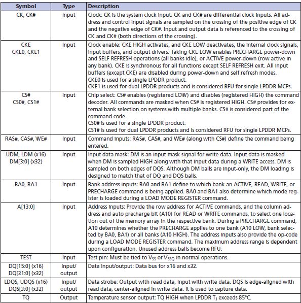
The chip uses a differential input clock signal. That means there is a CK as well as its complementary signal CK# going to the chip. This strategy is used in high speed interfaces. These 2 signals have to be generated by the FPGA using its PLL and supplied to the DRAM. The point where the CK and CK# cross each other is considered the clock edge.

Commands to the memory are registered on each positive edge of CK. Data is transferred on both positive and negative edges of DQS(Data Strobe). DQS acts as an output for the DRAM when reading data; and as an input when writing to DRAM. Two DQS transitions occur per clock cycle enabling double data rate access.
Below is a functional block diagram of the DRAM: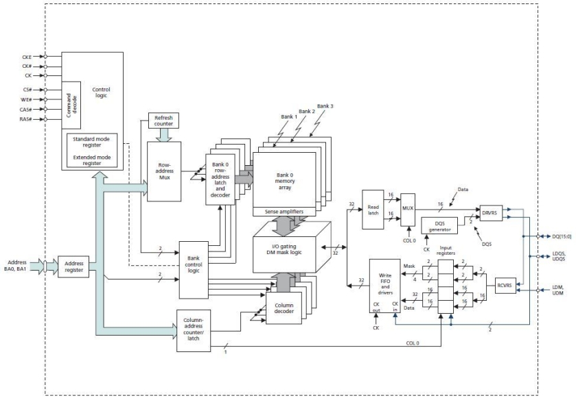
The data is stored in a ‘memory array’. It is exactly what you think it is: elements arranged in rows and columns. Each element in the case of our chip is 16bits in size. The memory is organized as banks for performance advantages. Each bank consists of 8K rows and 1K columns. There are 4 such banks. Thus the size of the memory is 4(banks) x 1K(columns) x 8K(rows) x 16bit(element) = 512Mbit.
Thus we need 13bits to address rows, 10bits to address columns and 2bits to address banks. The chip has only 13 address pins in total – they are used to specify row or column addresses depending on the status of other signals. Two pins BA0 and BA1 are dedicated for bank addressing. 16 pins DQ[15:0] are used as data pins.
Why is it split into 4 banks? The memory is designed such that only 1 row in a bank can be active at a time. An active(open) row is one which can be read or written to currently. Once you are done with a particular row, you have to close it after ‘precharging'(closing) it – this seals the contents of the memory. The action of activating and closing a row takes a lot of time(increased access time). Thus it is important to minimize the number of openings and closings during operation. Thus The provision of 4 banks allows 4 rows to be active simultaneously reducing the access times.
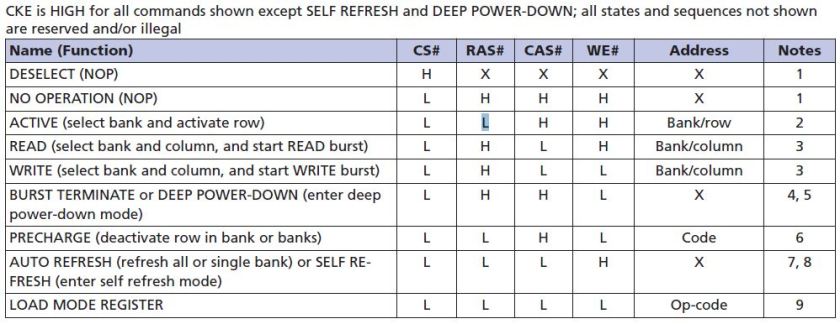
RAS# is known as row address strobe. When opening a row, the 13bit row addr is specified and RAS# is made LOW. Once the row is opened, you can access the columns of that row. This is done by specifying the starting column addr, burst length and making CAS# LOW. WE# is used to specify when it is a write operation.
The double data rate is achieved by prefetching 2 elements from the memory array and outputting one element each half cycle. This is taken care by the chip itself. The chip has inbuilt circuitry to automatically refresh the memory without any intervention.
The chip also has TCSR(temperature compensated self refresh). The leakage rate of the memory cell depends upon chip temperature – higher the temperature, refresh rate needs to be increased. The chip has inbuilt temperature sensor which helps in adjusting the refresh rate.
The memory controller:
If you have seen the timing diagrams in the datasheets, we see that we need precise signals to reliably communicate with the DRAM and achieve maximum bandwidth. Writing the logic to communicate with the chip is very complex as it involves so many protocols to be followed for the different operations.
Fortunately, the Spartan 6 FPGA has inbuilt hardwired memory controller block(MCB) which can be used to interface with different kinds of memories DDR2, DDR3, LPDDR etc. The Core Generator tool can be used to generate a memory controller which uses the hardwired MCB plus some FPGA fabric. The thus generated MCB module provides a simple interface to the user which hides the complexity involved in memory communication. The user logic talks with this module to read/write data to LPDDR.

The MCB supports multiport configuration. We shall deal with a single port configuration for our application. It is a 32bit bidirectional port named port0. Though our memory is a 16bit memory, the MCB provides a 32bit interface which means that the user logic sees the LPDDR as having addresses holding 32bit words. port0 has 3 ‘paths’ – the command path, read path and write path. These paths are nothing but FIFOs of specific depth. The command, write and read FIFOs are 4, 64 and 64 elements deep respectively.
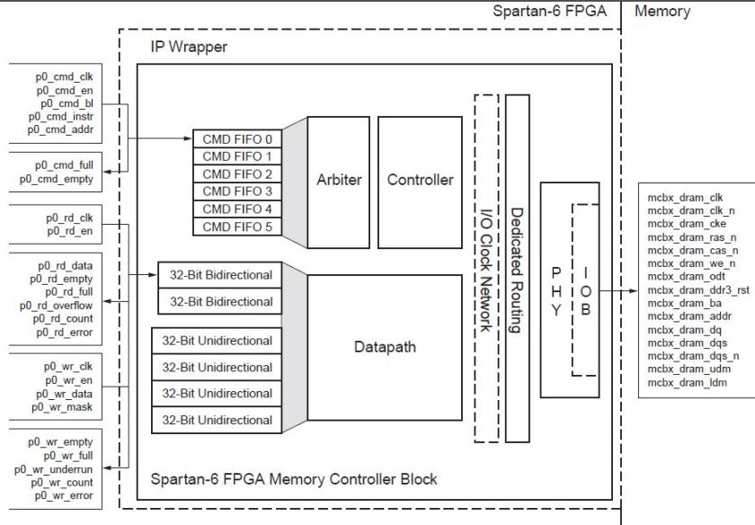
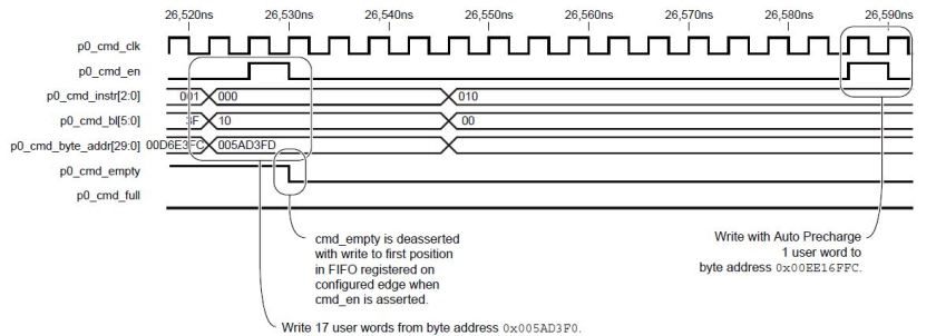
The command FIFO holds the operation that should be performed on the memory eg. read,write,refresh etc. Along with the operation, the starting (byte)address to be accessed and the burst length(bl) is also loaded. The MCB sees the elements loaded into the command FIFO and drives the necessary signals to the memory. There is the cmd_clk and cmd_en signals as well as cmd_empty and cmd_full to know the status of the cmd FIFO. The [2:0]cmd_instr tells the operation – 000=write, 001=read etc.
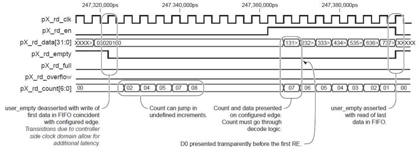
The Read FIFO holds the data that has been read from the memory. These signals again follow the same pattern as cmd FIFO. The user logic reads data from the FIFO. rd_empty and rd_full tell whether the FIFO is empty or full. rd_overflow tells if the FIFO has overflown with data from memory; thus its important to load read commands into the cmd FIFO keeping in mind the status of the Read FIFO. [6:0]rd_count tells how many elements are there in FIFO (but it is not updated immediately after data is read into it. so rely on rd_full and rd_empty to know exact status).
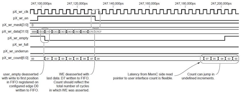
The write FIFO is not very different from the read FIFO. The only difference is that it contains a wr_underrun signal which is asserted if you are trying to write more elements to memory than is available in the FIFO. Thus the cmd FIFO should be loaded only after sufficient number of elements are present in wr FIFO to satisfy the burst length. There is also this wr_mask which can selectively write only specified bytes in the 32bit word to the memory.
For complete understanding of the MCB I highly recommend going through ug388, ug416 and also if needed ug086 datasheets. I have omitted a lot of explanation for the sake of brevity.
Clocking the MCB:
The core gen tool automatically adds & configures the necessary circuitry to provide the clocking. Its good to understand what is happening.
Now, our LPDDR chip needs a differential clock as explained before. We shall choose our clock speed to be a nice number like 100MHz (though the memory can run upto 166MHz). Thus the maximum transfer rate possible is bandthwith = 2*100M*2bytes/s = 400MB/s.
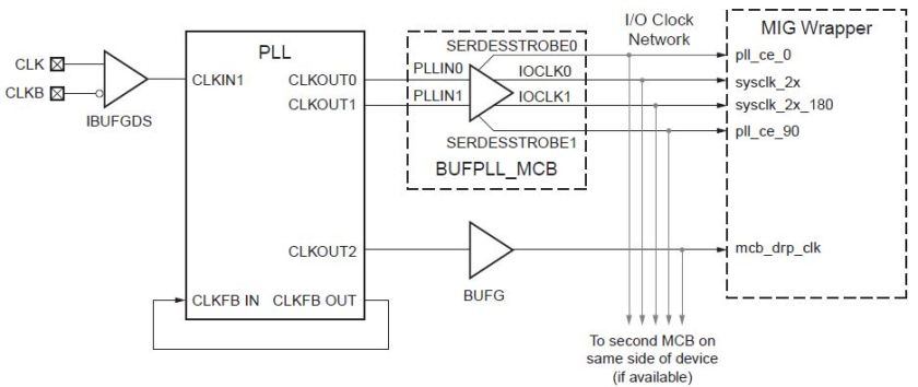
We have a 100Mhz crystal clock source for the FPGA. But this clock may have many imperfections like jitter, duty cycle etc. For a reliable communication with the memory we need perfect timing. We use a PLL(ADV_PLL primitive) to synthesize the required clock and also reduce the jitter in the crystal source.

The PLL can produce 6 simultaneous outputs of customizable frequency, phase, and duty cycles. The main parameters of the PLL are D, M and O0-O5.
output frequency F(Oi) = Fin*M/(D*Oi)
O0 and O1 are ‘eventually’ used for generating CK and CK# respectively. O2 is used as user clock. O3 is used as a calibration clock while O4 & O5 are left unused. We keep M=4, D=1, O0=O1=2, O2=4, O3=8. This gives F(O0) = F(O1) = 200Mhz; F(O2) = 100MHz; F(O3) = 50MHz.
The PLL block is followed by a BUFPLL_MCB block. This block is used to generate additional clocks from the PLL’s output to drive the MCB. This block simply buffers the 2 200MHz clocks and passes it on to the hard MCB block. It also divides the 200MHz clock to generate two 100Mhz clocks 90degress out of phase pll_ce_0 & pll_ce_90. These two signals pulse High on every other clock cycle of the 200MHz clocks. It is used for double data rate transfers in the I/O blocks.
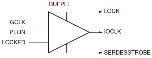
The BUFPLL_MCB contains 2 BUFPLL blocks shown above. The BUFPLL_MCB also pass on the calibration clock to the MCB.
Finally, the hardwired MCB module itself divides down the two 200MHz clocks to provide a differential 100MHz clock to the memory. The 200Mhz clocks also drive the MCB itself. The calibration clock is used to synchronize the calibration module inside the MCB to the 200MHz domain.
Getting to work:
Now I think you would have a good idea of the working of the memory as well as the MCB system. Its essential that you have a read of the datasheets I have mentioned before to get a clear understanding.
We can start with our design now. Numato labs has provided a good tutorial to use the core gen tool to generate a MCB design for the MimasV2 board. We need to modify and add to the generated design for our application. Hence follow the tutorial as it is; we shall start working on our design from next tutorial.
You should find this link helpful for adding the PATH environment variable (you will need it while following the Numato tutorial).
Cheers!
Anirudh
